
Since the inception of satellite communications (SATCOM), the parabolic reflector antenna has been the”go-to” technology that has enabled reception (downlink) and transmission (uplink) of data using radio frequency (RF) signals from Earth-based SATCOM terminals.

While these ubiquitous “dishes” have provided a highly effective and efficient means for RF transmission from fixed points on the ground, the traditional parabolic antenna design does not lend itself as easily for...
1) airborne
2) maritime
3) on-the-move ground vehicle
4) ultra-light “backpackable” communications due to the volume and space required for the dish shape, along with the need to mechanically steer the dish RF beam on a continuous basis toward the satellite.
To address this issue, a growing number of companies are in the midst of developing flat panel satellite communication antennas, providing a low profile (flat) aperture with an electronically steerable beam that can be more easily adapted (affixed) to moving platforms. Additionally, flat panel antenna companies are pursuing a number of different technologies that can be categorized into two basic design approaches:

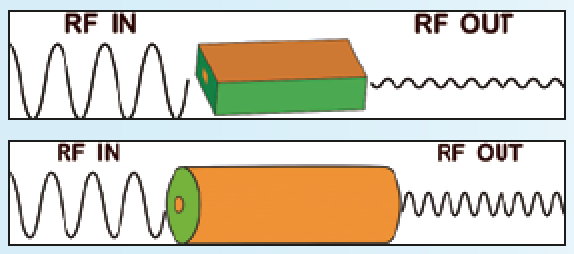
1) waveguide-based structures
2) printed circuit board (PCB) technologies.
Both technologies have distinct advantages and disadvantages for SATCOM.
Performance and Loss
Antennas designed with conventional waveguide-based structures are high-performing and are less lossy than PCB technologies.
Waveguide is air-filled like a vacuum, so typically there’s no dielectric material for the signal to travel through or to create losses — waveguide is effectively lossless. Conventional waveguide antennas are considered familiar to many operators as these antennas use the same performance and loss calculations as reflector-based antennas.
PCB technologies are high performing and easily scalable, but they also operate with significantly more loss characteristics than waveguide structures — so much so that most operators don’t anticipate the signal degradation experienced with PCB-based antennas, particularly at high frequencies. The reason is that PCB is a filled material, so losses occur as a signal travels through the dielectric materials used for fabrication.
An analogy to losses using waveguide versus PCP materials would be signal loss in a coaxial cable. If a sine wave is introduced into a coaxial cable on one end, then at the other end the loss is observed as the sine wave is decreased on magnitude and also shifted in phase.
Losses generally are a problem when a strong, steady signal is a requirement, such as for SNG (satellite news gathering) or streaming video. For general data transmission, signal degradation will impact performance, but to a manageable extent. These losses are accounted for in the link budget, which is determined during the system design process.
Size and Weight
A clear disadvantage with conventional waveguide-based structures is that they tend to be large and heavy. In order to produce adequate gain for use in satellite communications, the resulting number of power dividers and antenna elements make for a structure that is heavy and often quite thick compared to typical user expectations.
The size of a waveguide-based structure will be determined by the application and performance requirements. A smaller waveguide-based terminal will work well with backpack comms-on-the-pause uses, but a much, much larger terminal will be required to maintain enough gain and bandwidth for a large aircraft with numerous simultaneous users.
That said, PCB structures are much more compact than waveguide based systems, and though the materials tend to be heavier than conventional FR-4 circuit board material, they typically are more in line with the expectations of the end user when it comes to flat panel technologies.
The downside to FR-4 is that it only works below 1000 MHz. SATCOM requires dramatically different circuit board materials, including ceramic-type materials, to operate at SATCOM frequencies.
For a backpack-based (manpack) solution, a PCB-based structure with a given performance expectation likely will weigh less and be more flexible in terms of scaling or using multiple subarrays. That said, a waveguide-based manpack antenna may be higher performing depending on the environment, but bulkier and heavier to carry.
Form Factor and Scalability
The dielectric constant in PCB structures can range between 3 and 10 for common high frequency materials and this will result in smaller PCB structures.
Therefore, as PCB structures operate at shorter wavelengths, PCB structures are inherently smaller. This makes PCB structures, particularly feed networks, significantly simpler to scale up for a larger terminal, or scale down for a smaller terminal when sub arrays are used.
PCB structures are rigid, but they’re less rigid than waveguide-based structures. For a PCB structure to conform to a required shape, such as the top of the fuselage of an aircraft, flexible circuit material can be used such as a membrane, and that enables PCB structures to be shaped for conformal applications.
Air-filled waveguide structures have a dielectric constant of ~1 and there is no miniaturization of the waves. Therefore, adding subarrays to increase size is conceptually easy, but that, in combination with the required feed network, may prove to have weight and size characteristics that would inhibit this approach.
As waveguide structures are rigid, multiple waveguide-based subarrays would be needed for a conformal application and each subarray would share a common feed network. Shaping waveguide-based subarrays for a conformal application is challenging as well as heavy and bulky.
Manufacturability
Because of the significant number of power dividers and antenna elements needed to produce adequate gain, waveguide-based structures are typically complex to manufacture.
Each antenna element, such as a slot, has a bandwidth requirement that is difficult to achieve if the antenna is designed for structural simplicity or ease of manufacturability. Waveguide-based structures require significant engineering and expert manufacturing supervision, as well as well-trained manufacturing labor. While efficiencies of waveguide-based technologies tend to be more easily achieved than the PCB-based alternatives, the inherent designs tend to require shapes that typically require machined metal fabrication, making them much heavier.
PCB technologies have been used in commercial electronics for many years and, as such, offer lower costs per unit and are designed for high volume manufacturing. It’s a natural progression to take circuit board technologies and apply them to the SATCOM industry, as PCBs have evolved to a somewhat more simple manufacturing process and are conducive to high volume manufacturing. PCB manufacturing also requires less hands-on labor; however, significant engineering and expert supervision is required to ensure precision manufacturing.
PCB material choices can create difficulties. Materials suitable for high frequency transmission, such as Ka-band satellite communications, are not low cost when compared to materials used for commercial electronics circuit boards, such as FR-4. Additionally, the materials suitable for high frequency applications are also difficult to manufacture into multi-layer circuit board structures.
Also, as commercial electronics have used PCBs extensively in product design, the availability and manufacturing tolerances are well understood. Difficulty for the antenna designer is often not in finding a PCB fab house, but rather in finding one with experience in working with the specialized materials required for satcom. This can include both the ability to manufacture and engage in the appropriate conduct testing.
Frequency Flexibility
A significant challenge in using array antennas for SATCOM applications is the frequency dependence of each array — this dependence means that flat panel antennas — regardless of waveguide or PCB structure — are not able to change bands to operate on vastly different networks. A Ku-band flat panel terminal only operates in Ku-, and a Ka-band terminal only operates in Ka-.
Arrays always have a limited bandwidth, hence the frequency dependence, and this creates the challenge of designing an array’s bandwidth to be wide enough for SATCOM. In addition, the spacing of the elements affects the overall terminal pattern and a typical array terminal needs to have the elements spaced at half a wavelength to one wavelength apart.
For applications requiring frequency changes — such as an SNG truck that broadcasts through multiple networks — the operator would be better served with a parabolic antenna with quick-change RF kits, than with a fixed-band flat panel terminal. Many parabolic antennas are multi-band as long as the operator can change the RF equipment, and this enables significant flexibility when required.
www.avltech.com/

Ian Timmins, Ph.D., is the Principal RF Engineer at AvL Technologies. Prior to joining AvL, Ian was VP of Engineering for Optical Cable Corporation’s Enterprise and Harsh Environment lines of business. He also previously held technical roles with Dell Computer Corporation, Cisco Systems and COM DEV Space Group. Ian holds a Ph.D. in Electrical Engineering and is an adjunct professor with Western Carolina University.