Satellites—those man-made objects that orbit the Earth—have a variety of different uses, from broadcast entertainment and telephone communication to weather prediction and navigation services.
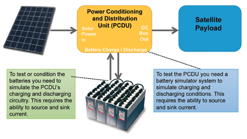
Figure 1. Shown here is a simplified block diagram of the power flow of a satellite. The arrows going in both directions indicate the need for a solution that can source and sink power for testing.
While their uses may differ, all satellites share a key requirement—the need for power. Satellites harvest their power from the sun via solar array or photovoltaic (PV) panels. However, because of the satellite’s spin and potential for the solar panels to be shaded, that power source is not constant. To compensate, the solar power is often supplemented with batteries that can be charged and discharged to provide a consistent power source to the satellite payload.
The job of controlling the power flow from the solar array panels to the batteries, and distributing a constant stable power source to the rest of the satellite, falls to the Power Control and Distribution Unit (PCDU). The job of ensuring the PCDU and satellite batteries perform as expected falls to the test engineer, and that’s no easy task.
While there are three primary options for addressing this challenge, each has its own shortcomings that make it less than ideal. Fortunately, technology advances are now bringing an alternate option to light and it promises to address all the key requirements for satellite power test.
Understanding The Test Requirements
When testing a satellite PCDU or performing satellite battery testing, there are a number of requirements that must be met; perhaps the most important of which is for the solution to be able to source and sink (load) power. This is critical since both the satellite batteries and battery management electronics in the PCDU have bi-directional power flow test needs (Figure 1). For battery testing, for example, source power is needed to charge the batteries, while load power is needed to discharge the batteries. To test the PCDU, being able to simulate the charge and discharge of the batteries is critical.
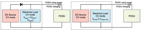
Figure 2. The non-overlapping source-sink solution with deadband is shown on the left, while the overlapping source-sink solution is on the right; both are suitable for PCDU testing.
Another requirement for satellite power test, when testing or conditioning batteries, is for the solution to operate in voltage (CV) and current (CC) mode. For testing the PCDU, the solution should seamlessly transition between sourcing and sinking current without any disruptions or deadbands in the output. The ability for the solution to handle various load/Device-Under-Test (DUT) impedance conditions is also critical, as is the need for protection features, limit settings and a fast reaction time to questionable test conditions. Protection, in particular, is critical for a number of reasons; namely, because during satellite power test the batteries can explode and the DUT is typically very expensive and hard to replace. Having a source-sink solution that is able to tightly regulate its voltage and current, and react quickly to questionable test conditions helps minimize this risk.
Finally, the test solution must be able to deliver reasonable performance levels (e.g., output noise levels and output level accuracy) to meet DUT test specifications, and be of a reasonable size and weight so that it can be easily integrated into a standard size test system.
Satellite Power Test Options
Three possible source-sink solution options for satellite power test include a non-overlapping source-sink solution with deadband, an overlapping source-sink solution and an integrated source-sink solution. Each option has its pros and cons.
The non-overlapping source-sink solution with deadband combines a DC source and electronic load, as shown in Figure 2 below. A diode may also be needed to prevent current from flowing into the DC source.
The solution provides a stable output, can handle dynamic load currents and covers a wide power range. It operates primarily in CV mode, making it more suitable for PCDU testing. Its key disadvantage is that due to the electronic load transitioning in and out of CV mode, it does not provide seamless, glitch-free operation. It is also quite complex, requiring the engineer to program and control two instruments (the DC source and electronic load). Additionally, an external instrument such as a digital multimeter or shunt, is generally needed to ensure accurate, gap-free measurements.
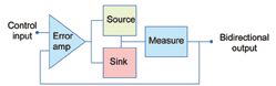
Figure 3. Shown here is the configuration of a single instrument test solution with integrated sourcing and sinking.
Like the non-overlapping solution, the overlapping source-sink option uses an electronic load and a DC source; however, the DC source is much higher power (higher current) and the electronic load is used in CC mode at a fixed level of at least the PCDU’s maximum source (charge) current (Figure 2). Because of this, it does not have a deadband area and can maintain a constant voltage level when the DUT current transitions between sourcing and sinking.
While the solution does deliver a reasonably transient-free voltage response with no deadband, its size is a huge drawback. The DC source that’s used has to be more than twice the DUT’s power level, which results in a rather large power supply. Also, as the load is always dissipating power, it has a large energy usage footprint. Making accurate current measurements is also challenging because the current is the difference of that between the electronic load and the DC source, meaning that the measurement uncertainty of each instrument must be combined. Moreover, to ensure the solution’s stable and predictable operation, custom hardware may be needed.
Although not depicted, battery testing requires a variation of the non-overlapping source-sink solution whereby the electronic load and DC source operate independently in constant current with voltage limits for limiting discharging and charging. Here, safety features are of primary concern and supplemental custom hardware is required over and above what protection features are built into standard electronic loads and DC sources.
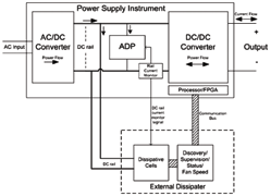
Figure 4. Shown here is a block diagram of a switching power supply design with source-sink capability achieved through the use of a bi-directional DC-to-DC converter, ADP and ED.
The last option, the integrated source-sink solution, provides two-quadrant operation. This means that the power sourcing and sinking operation are control by a single regulation loop (Figure 3 below). As a result, it offers seamless operation when transitioning between sourcing and sinking, as well as consistent performance and operation whether sourcing or sinking power, all without the need to dissipate large amounts of power.
Another key advantage is that the solution, with appropriate voltage and current controls, can be used equally well for testing satellite batteries and PCDUs. A key disadvantage is simply that it’s difficult to find an integrated source-sink solution that’s within a satellite’s power range (i.e., kilowatt and greater power levels).
Linear DC power supplies offer an architecture that supports two-quadrant operation, but become too large at satellite power levels. The architecture of a switching DC power supply, on the other hand, provides a small test system footprint, but it doesn’t easily support two-quadrant operation.
Overcoming The Disadvantages
Generally speaking, the most common approach for satellite power test is to use separate instruments for sourcing and sinking—as is the case with the non-overlapping and overlapping source-sink solutions—as the instruments are readily available. The shortcomings of these solutions can be overcome by employing an integrated source-sink solution; however, the challenge here is to find a viable one. Fortunately, a number of new technologies are now making that search easier. The technologies include a bi-directional DC-to-DC converter, and a patented automatic down-programmer (ADP) and external dissipater (ED).
The DC-to-DC converter uses technologies including synchronous rectification to give it bi-directional power flow capabilities. Adding a bi-directional DC-to-DC converter capability to a switching power supply allows any stored energy at the output between the two conversion stages of the power supply to be discharged. The patented ADP allows down-programming to be performed on the DC bus. Essentially, it monitors and sinks current whenever the DC bus voltage begins to rise. The patented ED expands the bus monitoring and current sinking capabilities of the ADP, although unlike the ADP it is external to the power supply. With the ED in place, the power supply is able to achieve full source sink or two-quadrant operation.
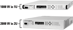
Figure 5. Agilent Technologies’ APS family of system power supplies comes in 1- and 2-kW power ranges, with the capability of being paralleled up to 10 kW. The family features two performance levels: the N6900 Series DC power supply, which is designed for ATE applications where high performance is critical, and the N7900 Series dynamic DC power supply, which is designed for ATE applications where high-speed dynamic sourcing and measurement is needed.
When used together, these technologies enable the creation of an integrated source-sink solution, based off of a switching power supply architecture, which is controlled by a single regulation loop (Figure 4). A prime example of one such solution is the Advanced Power System (APS) N6900 and N7900 family of system power supplies (Figure 5). These integrated source-sink solutions meet the solution requirements for satellite power test, while offering high precision and accuracy in an instrument-grade switching power supply architecture.
Using an integrated source-sink solution such as the APS offers a number of critical advantages over both the non-overlapping and overlapping source-sink solutions. To begin, whether sourcing or sinking current, the power supply uses a single regulation loop to control both. Consequently, the same specifications and performance are delivered regardless of whether the power supply is sinking or sourcing power. It also offers seamless glitch-free transitions between source and sink operation and does not waste large amounts of power. There is also less hardware and software complexity since there is only one instrument to connect the DUT to and control via software. Additionally, no custom hardware is needed. Furthermore, since it’s based off of a switching power supply architecture, the hardware size and weight is greatly reduced.
Solution Determination
While it’s clear that a source-sink solution is needed to properly test satellite batteries and the PCDU, determining which solution to use is complicated by the fact that each has its own set of disadvantages. Today, the non-overlapping and overlapping options are most commonly employed, but the integrated source-sink solution offers a much more advantageous option; assuming one can be found.
That’s where the development of a bi-directional DC-to-DC converter and patented ADP and ED technology have roles to play. These technologies have enabled the creation of an integrated source-sink solution in a switching power supply architecture. The solution meets all of the requirements for a satellite power solution, without any of the disadvantages of the other options—all of which is good news for any test engineer tasked with testing satellite batteries and PCDUs.

About the author
Ed Brorein is a marketing applications engineer with Agilent Technologies, helping customers using power products both in manufacturing and R&D. He joined Agilent (formerly Hewlett Packard) in 1979 and has worked as an R&D engineer, manufacturing engineer and marketing engineer in various roles. Over the years, Ed has been actively and deeply involved with the design, engineering and application of DC power products for testing of electronic devices and products. He received his BSEE from Villanova University in 1979 and an MSEE from the New Jersey Institute of Technology in 1987.