
An important determinant of spacecraft reliability is the fault tolerance of its power management and distribution (PMAD) system in a radiation environment.
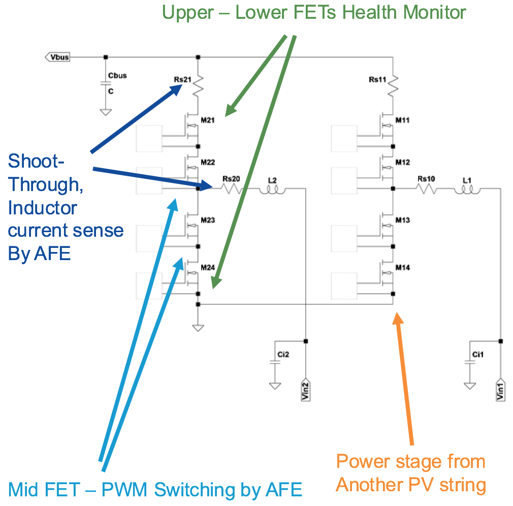 Figure 1: The DC/DC boost fault tolerant power stage.
Also advantageous is to reduce the footprint of a redundant PMAD system using ICs that offer a high degree of integration. These goals can be achieved with a new PMAD topology consisting of a series of metal-oxide-semiconductor field-effect transistors (MOSFETS) driven by a single analog front end (AFE) IC that implements sense and control interfaces to the power devices.
Taking this approach also requires a system design that alleviates parametric drift due to radiation effects on the AFE. This is accomplished by adding a radiation-hard FPGA that enables the AFE sub-system to run maximum power point tracking (MPPT) on multiple strings of photovoltaic modules while also delivering power to the main power distribution bus. Meanwhile, additional protection circuits manage power distribution to loads and to and from a battery unit.
A New PMAD Topology
The PMAD system must optimally transfer power from the input sources and manage all power transmission.
Key system components include DC/DC converters, protection circuits and a power transfer and fault management function that is partly local and partly remote. A footprint-reducing topology for these functions that uses photovoltaic (PV) module strings as inputs must ensure fast and accurate MPPT control to track varying angle, shading and/or temperature condition per string. This allows several boost DC/DC power converters to independently seek maximum power point (MPP) per string while driving the power distribution bus.
The topology also must ensure that voltages on input and output nodes and currents through each converter are monitored and used to control each DC/DC converter. Temperature must be monitored at key points and DC arc fault detector circuits should be used per string to detect arc on each high current/voltage rail where it could develop.
Control is performed digitally using the combination of an AFE to convert all sense lines to digital and to drive MOSFETs from digitally generated pulse width modulation (PWM), and an FPGA to implement DC/DC control, MPPT and power and safety management.
Topology of the Fault-Tolerant Power Stage Control
The DC/DC boost unit converter is implemented using a series connection of two n-channel metal-oxide semiconductor (NMOS) transistors for each high and low side. This ensures the controller can disable both high and low side paths in case of a short circuit developing in one of the four MOSFETs at the expense of some converter efficiency loss (see Figure 1 in the left column.) .
During regular switching periods, the uppermost and lowermost MOSFETs are on continuously, while the middle ones are switching. Switching is periodically exercising the uppermost and lowermost MOSFETs to verify their health state while the middle ones are turned on continuously. If shoot-through current or inductor current sensors detect a large change when moving from middle to uppermost and lowermost MOSFETs, a fault is identified, the power stage is disabled, and a redundant power stage is enabled.
The AFE can sense any inductor and shoot-through current. The shoot-through current measure is based on a difference measurement. First the switching is done with enough dead band to guarantee no shoot-through current and the peak current is measured. In the next switching cycle, the timing to be measured is applied and the peak current is measured again.
The difference between these values is a measure of the timing dependent shoot-through current. This measure is repeated several times and the controller low pass filters it to eliminate input or output transient influence.
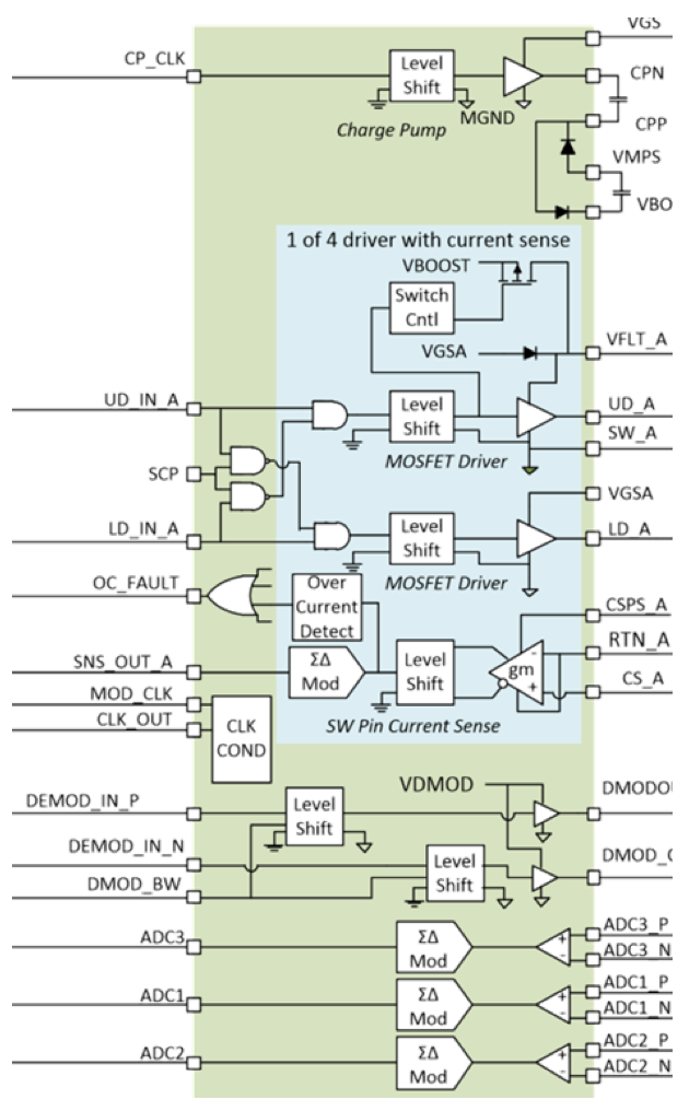 Figure 2: Microchip LX7720 motor controller block diagram.
The shoot-through current, together with a conversion efficiency measure (using input and output current and voltage sensing), is used by the FPGA-based controller to constantly fine-tune MOSFET timing in order to track the actual value and compensate for any long-term radiation or temperature-induced timing drift. This avoids needing to add a lot of margin for timing degradation and using a large dead time as in a classical design. The other alternative to classical design is to use a circuit that includes some loop-controlled delay in the gate drivers, but these circuits are more complex and expensive to build.
For better results, the MOSFET-driving capabilities of radiation-tolerant devices traditionally used in space motor control applications can be leveraged for the integrated PMAD AFE to compensate for all variation. The extra current sensor of these devices enables PMAD systems to compensate for all variation. Their capabilities are illustrated in Figure 2 using Microchip’s LX7720 radiation-tolerant spacecraft motor controller as an example.
Four high-side / low-side pairs of gate drivers are used to drive all 8 MOSFETS required to implement the two fault-tolerant power stages. The device’s internal charge pump is activated to turn permanently on the uppermost side’s MOSFETs connected directly to the rail (except when the estimation of the health of the system is done and MOSFETS change roles). Additionally, the device’s resolver driver outputs are employed to drive the primary of an isolated forward DC/DC converter to power an auxiliary circuit used for PV arc fault detection.
The next step is to combine the AFE with power line protection devices for power distribution. An example is Microchip’s LX7712 featuring a solid-state P Channel MOSFET switch and catch diode. It uses switch temperature to trigger an optional thermal shutdown and can be configured as a latch-able or fold-back current limiter. Multiple devices can be paralleled in a master/slave arrangement if an increased latching current limiter (LCL) class is needed.
The latch-able current limiters of these devices’ can be configured to latch in the off state due to a fault (operating as an LCL) or to attempt to restart in a hiccup mode operating as a retriggerable LCL (RLCL). A fault time integrating function remembers the cumulative effect of short fault pulses and should be configurable for a fixed duration or a duration that is a function of the voltage drop from line-to-load across the device.
In fold-back current limit mode the profile of the fold-back load current versus load voltage curve should be resistor-programmable. It should also be possible to configure the fold-back feature for bi-stable operation; applying an overload forces the current limit to a safe trickle level and, when the fault is corrected, the current limit returns to its normal level. This prevents “soft short” power dissipation situations.
Operating the AFEs
An FPGA is used to implement several state machines and must also run load on/off control, diagnostics and communication functions. Because the DC/DC converter source is a PV module or string, the associated control should be based on a slow/fast input voltage regulation loop approach. The fast loop implements a PID loop to regulate the input voltage of the boost DC/DC to a target voltage, and the loop uses the difference of the input voltage to target voltage to drive the DC/DC converter duty cycle. This loop limits duty cycle such that SOA of devices is met.
While the fast loop regulates the input voltage to a target voltage, the slow loop (MPPT state machine) dynamically determines that target voltage to reach MPP. One approach that can yield a very fast control for the slow loop is to use a PV model and minimum number of off-MPP experiments to determine directly the ideal PMM after a light, temperature or shading change happens. The MPPT response time of this method after an abrupt shading change is approximately 1 millisecond (ms, or 20 switching cycles) if the input filtering is not excessive. In case of partial shading, the control avoids large reverse biasing of the affected cell (hot spot suppression).
The shoot-through current/dead time optimizer should be designed to adjust timing of the high / low side MOSFETs for maximum efficiency while ensuring estimated shoot-through current is negligible and dead time is minimal. The value of the shoot-through current is a relative measurement as previously described and represents an averaged difference between the measured current at large margin and the estimated margin. The sense chain is limited to a known resolution. If the difference is smaller than that resolution then the timing does not yield shoot-through current and the loop can further reduce the dead time, otherwise dead time is increased.
Efficiency optimization is performed by changing the switching frequency and observing a measure of losses in the converter. The optimization space is a range of switching frequencies. This can be a discrete set for systems that cannot tolerate any switching frequency, or a frequency range. The optimizer starts from the largest frequency and uses a steepest descent algorithm.
ICs traditionally used in actuator control are poised to help solve the challenges of implementing a PMAD AFE used in space. They enable developers to build systems that dynamically perform MPPT while tracking temperature- and/or radiation-induced drift of the power stage and gate drivers and optimizing dead time and conversion efficiency.
A radiation-hard FPGA and a group of LCLs/RLCLs using power line protection ICs complete the system, delivering PMAD fault protection through a topology that can be implemented in a small footprint.
www.microchip.com/

Dr. Sorin Spanoche is a system architect at Microchip Technology, leading the architecture definition for mixed-signal high reliability IC products. With 30 years of experience in the industry, Dr. Spanoche is an expert in analog and mixed signals circuits and IC design (low power/noise, sensors, power, telecommunications, RF), algorithm design, digital architecture, system specification and architecture design for mixed signal systems.