
The rapidly increasing use of gallium nitride (GaN) technology to power solid state amplifiers is well known in the market. This article discusses why the change is occurring and whether there is a place for the older gallium arsenide (GaAs)-based amplifiers.
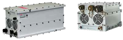
Left, CPI Model 7720H 100W C-band GaAs BUC
CPI Model 471H 100W C-band GaN BUC, right
From the early 1980s until just a few years ago, gallium arsenide (GaAs) field effect transistors (FETs) were the mainstay of the solid state high power amplifier (HPA) industry for radio frequency (RF) transmission.
Invented more than 30 years ago, the GaAs FET quickly gained acceptance over silicon-based devices due to its superior efficiency and ability to operate at much higher frequencies. In similar fashion, GaN FETs are now rapidly supplanting GaAs FETs for almost entirely the same reasons: better efficiency and the ability to operate at even higher frequencies. GaN FETs also outperform GaAs FETs in other key metrics, such as maximum temperature, gain, power handling, size and weight.
The adoption of GaN devices is occurring at a rapid pace, with foundries around the world racing to create new GaN devices. As a result of GaN technology’s superior performance (when compared to GaAs) in almost every attribute critical to the satcom market, research and development funding for solid state amplifiers is almost exclusively directed toward GaN efforts. This migration to the new technology has been surprisingly quick, given the traditional product cycle lengths in the satcom industry.

A typical example of the reasons for the preference of GaN technology is demonstrated in Table 1 on the following page.
At Ku-band, the results are also striking when comparing GaAs versus GaN. For the 40 W BUC comparison depicted in Table 2, GaN is again better by every key measure.
For Ka-band, the advent of GaN technology has enabled the design and manufacture of a 160 W amplifier, which provides four times the output power of the previous generation of GaAs =========== characteristics of this more powerful CPI amplifier are
as follows:
• Provides up to 100 watts of linear power over selected bandwidths (from 500 to 2500 MHz) within the 27.5 to 31.0 GHz frequency band
• Multiple bands available (Multiple LOs ; selectable with 1.0 GHz bandwidth)
• Multiple L-band input signal options for instantaneous 2.5 GHz output
• Designed for satellite uplink applications
• Suited for SATCOM-On-The-Move / Pause (SOTM/P), VSAT, antenna-mount and In-Flight Entertainment/Communications (IFEC) applications
The reasons why GaN is frequently superior to GaAs lie in the electrical properties of the materials, as illustrated in the following chart showing the three types of materials that have been used to manufacture FETs for HPAs used in satcom uplink applications, i.e., silicon (Si), gallium arsenide (GaAs) and gallium nitride (GaN).
The first row of Table 3 compares the three types of FETs for relative permittivity (also known as the Dielectric Constant), or the impedance to RF currents. A higher number represents greater impedance, while a lower number represents lesser impedance. In terms of performance, the rate of signal loss is higher where impedance is greater. GaN is the clear winner here.
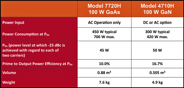
Table 1.
The second row, band gap, expressed in electron volts, is the energy range where no electrons can exist. It is also the energy required to promote a valence electron bound to an atom to become a conduction electron, which is free to move within the crystal lattice and serve as a charge carrier to conduct electric current. The lower the number, the less voltage it takes to start the movement
of electrons.
As illustrated in Table 3, GaAs amplifiers make very strong semiconductors due to their small band gap and superior electron mobility, but these characteristics also make them weaker candidates for higher frequency and higher temperature operation compared to GaN-based products. Gallium nitride’s band gap characteristic allows for operation at higher voltage. As the satellite industry is trending to progressively increased frequencies that require more power due to rain fade issues, GaN is by far the most promising material among the three.
When electron mobility, meaning the ease with which electrons can move through the semiconductor, is examined, as in row three, it is clear that GaAs technology is superior. High electron mobility results in a lower noise amplifier. For this reason, GaAs technology is still used in those applications where managing noise level is critical, such as in Low Noise Amplifiers (LNAs) or pre-driver stages. At the power booster stages, noise is less critical and provides the opportunity for GaN technology, with the already mentioned advantages in various parameters.
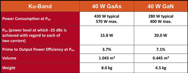
Table 2
The critical electric field characteristic, expressed in megavolts per centimeter in the fourth row of the table, is also a measure of robustness. It measures tolerance against electric field stress. In this particular measure, the higher the number, the more robust the material is. GaN’s higher rating indicates that GaN technology and materials are more tolerant to higher voltage operation than the GaAs equivalent.
The thermal conductivity comparison shows a superior ability by GaN and silicon to handle higher power than GaAs. And in the final comparison in Table 3, charge density measures the number of electrons that are available to charge per given volume: a higher number results in more output power per unit, resulting in a component and thus a smaller amplifier.
In the end, the measurements in the table demonstrate that GaN amplifiers handle heat, voltage and electric fields better; are more efficient; and can operate at higher frequencies while providing more output power.
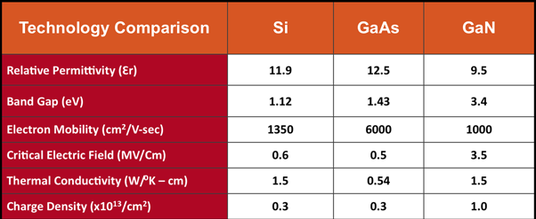
Table 3
GaN amplifiers are also superior to GaAs amplifiers when looking at overall system costs. Although individual GaN parts may have higher initial cost, overall cost reductions at the amplifier level are achieved due to better prime power efficiency and smaller size, enabling the amplifier supplier to incur less expense related to sheet metal, heatsinks and power supplies. Additionally, the cost of GaN MMIC parts has been trending lower over the last 10 years. These cost reductions are due in part to:
• Process improvements enabling better yields
• Increase in user demand (volumes)
• Increase in competition among device manufacturers
As an example, Communications & Power Industries (CPI) has seen a 50 percent reduction in the cost of 120 W C-band GaN devices between 2005 and 2014. These cost efficiencies are primarily driven by government funding of process improvements at the foundry level, with similar cost reductions occurring for GaN-based components and materials in the Ku- and Ka-band frequency ranges.
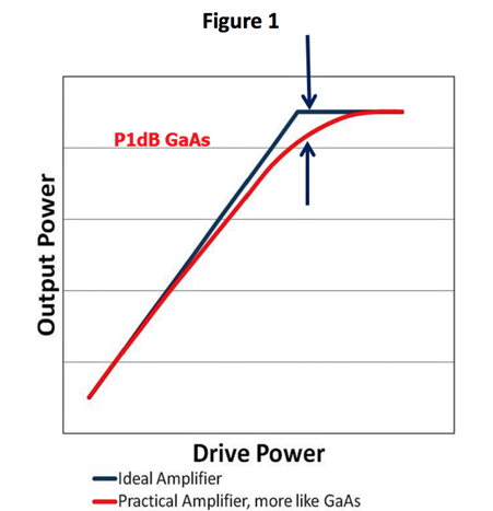
From a user or operator standpoint, RF performance is a principal measure for determining what amplifier technology should be selected. Users who compare GaAs to GaN often attempt to identify a common point of operation to make an equal comparison. The most common point chosen is the P1dB point, because almost every GaAs-based solid state amplifier or BUC produced in the last decade was specified with a performance at the P1dB point. However, due to the inherent differences between GaAs and GaN technologies, this P1dB point is not an accurate comparison metric, nor is it an accurate representation of the linear power capability of the GaAs-based amplifier.
The power at the P1dB point is occasionally misinterpreted as a measure of linear output power (or Plin). In practice, the P1dB mathematical metric is not relative to the ability of the device to transmit unimpaired signals. Rather, it is simply the point on a transfer curve where the gain has dropped 1 dB due to compression (see Figure 1).
To successfully transmit low bit-error-rate (BER) signals for most typical uplink applications, the user must operate below this P1dB point. For GaAs technology-based amplifiers, this operating point (to transmit low BER signals) has typically been at 3 dB below the theoretical P1dB point. Unfortunately, P1dB is used so frequently in the product marketing material that it is frequently confused with true linear power.
Linear power is more correctly defined as the point on the transfer curve where a meaningful parameter is reached. Such parameters are intermodulation (IM), spectral regrowth (SR), noise power ratio (NPR) or error vector magnitude (EVM), all of which have a real impact on the transmitted carrier or the adjacent channels which can be impaired. Adding to the confusion is the fact that some (but not all) GaN devices have a more gradual (softer) transfer curve than most GaAs devices.
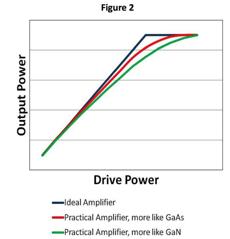
This soft curve can falsely depict GaN devices as having a lower linearity, as the artificial P1dB metric is lower (See Figure 2). In fact, GaN devices have relatively superior efficiency and power, such that the linear power performance is actually better for GaN technology than GaAs technology.
The most common parameters where this can be seen are (see Figure 2):
• IM (2-tone Intermodulation)
• SR (Spectral Regrowth)
• NPR (Noise Power Ratio)
• EVM (Error Vector Magnitude)
As a result of the inherent differences in the measures of GaAs technology versus GaN technology, as well as the resulting performance parameters that are key measures for performance, Satellite uplink operators and companies, such as CPI, are moving away from specifying P1dB on any Earth station amplifier product. Instead, they are simply stating the true linear power required based on IM, SR, NPR or EVM.
CPI Model B5KO 160W Ka-band GaN SSPA/BUC.
The following observations are clear when directly comparing the two technologies:
• GaN technology has enabled much higher output power and prime power efficiency than GaAs can achieve.
• GaN amplifiers are smaller and lighter than GaAs.
• The cost of GaN amplifiers is lower than GaAs amplifiers due to savings in the cost of housings, heatsinks and power supplies.
• The P1dB metric is being replaced (especially for GaN products) by the more meaningful linear (Plin) measure based on Intermodulation, spectral regrowth, noise power ratio, or error vector magnitude depending on the application.
To learn more about CPI’s full line of GaN based SSPAs, as well as amplifiers using TWTA and Klystron technology, please visit our website at www.cpii.com/satcom or download the CPI mobile app for Android or iOS.
While CPI endeavors to provide the most up-to-date and relevant information available, CPI makes no representations or warranties, expressed or implied, about the completeness, accuracy, reliability, suitability or availability with respect to the information, products, services, or related graphics contained herein for any purpose.